Highlights
Jun 8, 2018
University of Chicago
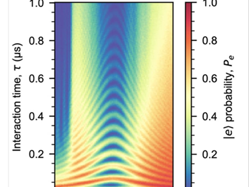
Quantum control of surface acoustic wave phonons
K. J. Satzinger, Y. P. Zhong, H.-S. Chang, G. A. Peairs, A. Bienfait, Ming-Han Chou, A. Y. Cleland, C. R. Conner, E. Dumur, J. Grebel, I. Gutierrez, B. H. November, R. G. Povey, S. J. Whiteley, D. D. Awschalom, D. I. Schuster, A. N. Cleland
The University of Chicago MRSEC has used super-conducting circuits and piezo-electricity to manipulate single phonons in a surface acoustic wave resonator (SAW).
Jun 5, 2018
Northwestern University
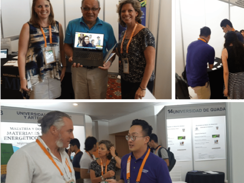
NSF-MRSEC Booth at the International Materials Research Congress
Following a successful inaugural year in 2016, a NSF-MRSEC booth was again featured at the XXVI International Materials Research Congress (IMRC) in Cancun, Mexico on August 19-25, 2017 to increase awareness, promote international collaboration, and broaden participation from traditionally underrepresented groups in the National Science Foundation Materials Research Science and Engineering Center (NSF-MRSEC) program. Dr. William Kung (Northwestern University), Ms. Michelle McCombs (Ohio State University), and Ms.
Jun 5, 2018
Northwestern University
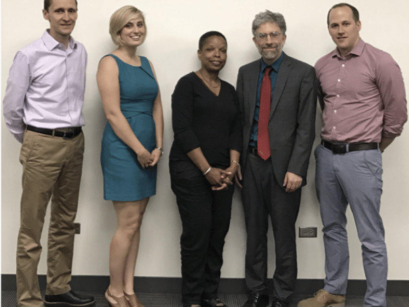
Research Experience for Teachers
Since its inception in 1992, the NU-MRSEC has offered the Research Experience for Teachers (RET) program each summer to middle-school, high-school, and community-college teachers with the principal goals of engaging them in research, developing a network of scientific colleagues, learning about new scientific and technological developments, and transferring this knowledge to the classroom. Concurrent with their summer research, teachers develop a related curriculum project to be implemented in their classrooms and shared with colleagues and administrators.
Jun 5, 2018
Northwestern University
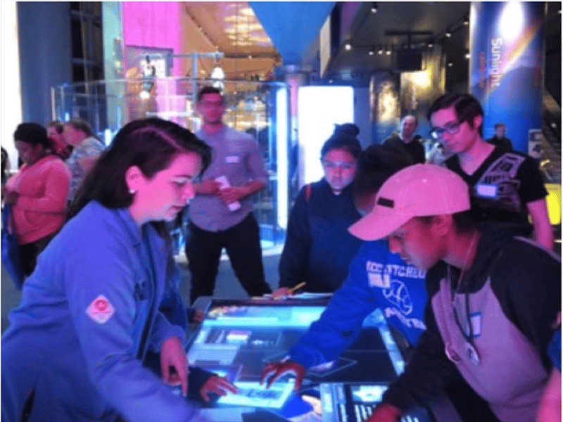
HerStory at the Chicago Museum of Science and Industry
In collaboration with the Chicago Museum of Science and Industry, HerStory is an outreach event that encourages young girls, particularly underrepresented minorities, to pursue science in academia and beyond. The event agenda includes a massive scavenger hunt at the museum that featured exhibits of famous female scientists in each wing of the museum. Volunteers and young women from across the Chicagoland area participated in the event.
Jun 5, 2018
Northwestern University
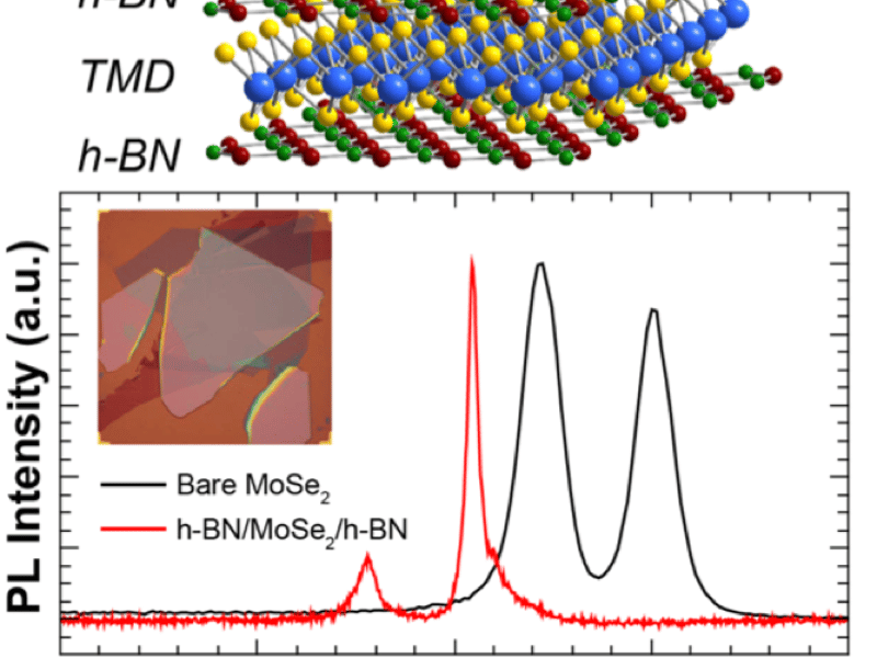
Encapsulated 2D Heterostructures for Enhanced Layered Optoelectronics
Two-dimensional (2D) layered materials have many features suitable for optoelectronic devices, but poor quality substrates can degrade optical properties. By encapsulating a monolayer semiconductor in layers of atomically-thin hexagonal boron nitride, a nearly pristine environment can be achieved free from surface roughness and defects of typical substrates.
Jun 5, 2018
Northwestern University
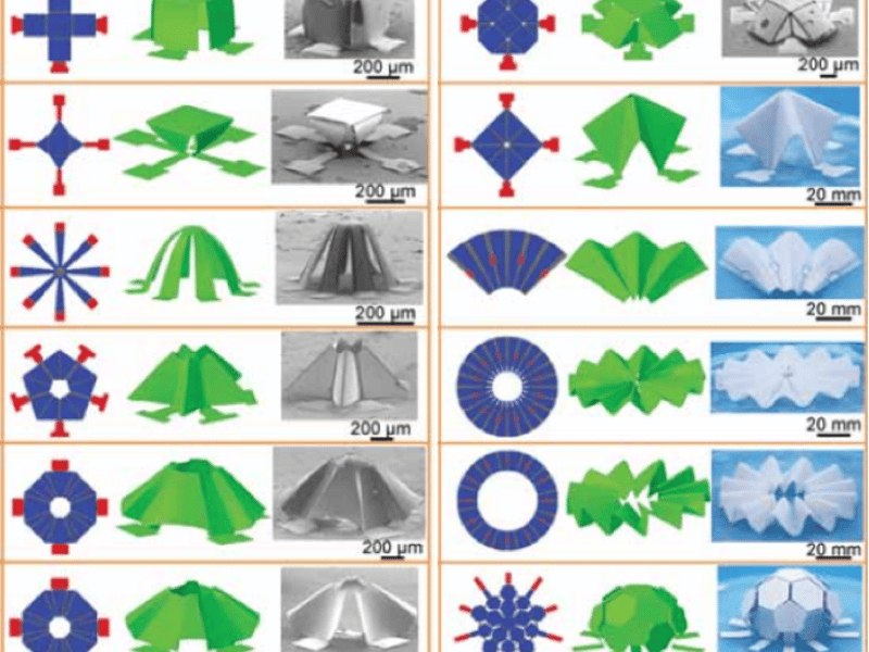
Controlled Mechanical Buckling for Origami-Inspired 3D Microstructures
A new strategy has been introduced to exploit mechanical buckling for autonomic origami assembly of three-dimensional (3D) microstructures across a wide range of material classes, including soft polymers and brittle inorganic semiconductors, and length scales from nanometers to centimeters. The engineered folding creases are created through spatial variation of thickness in the initial two-dimensional structures.
Jun 5, 2018
Northwestern University
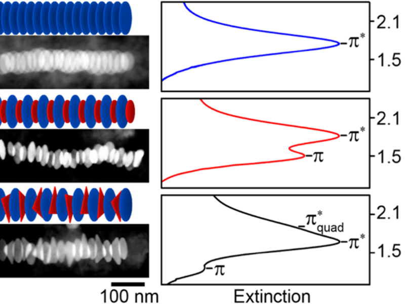
Tuning Optical Properties with DNA-Linked Gold Nanodisk Stacks
Recent advances in gold nanoparticle synthesis combined with functionalization with DNA linkers has enabled the self-assembly of stacks of gold nanodisks in which the optical spectra can be tuned and modulated by controlling the stack structure (e.g., particle spacing, arrangement, and stack length). The figure shows three possible arrangements of the particles, and the corresponding spectra that are associated with the plasmon resonance excitation in the stack.
Jun 5, 2018
Northwestern University
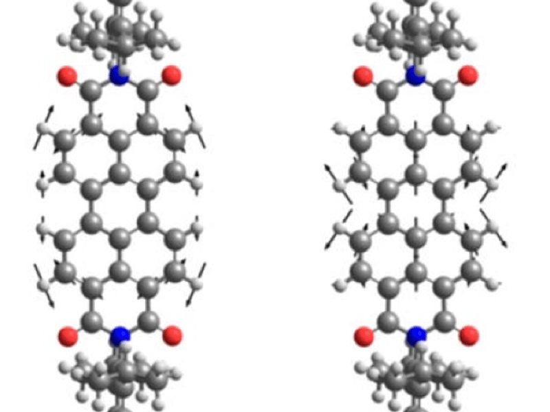
Probing Intermolecular Interactions with Intramolecular Resolution
At the nanometer-scale, the surface area to volume ratio increases substantially compared to bulk materials. Consequently, methods for functionalizing and passivating surfaces can play a dominant role in determining the properties of nanomaterials. Of particular interest are self-assembled monolayers of organic molecules that have been widely used to control the electronic, optical, chemical, and frictional properties of nanomaterials in a range of applications.
Jun 5, 2018
Northwestern University
High Performance Heterojunction Oxide Thin Film Transistors
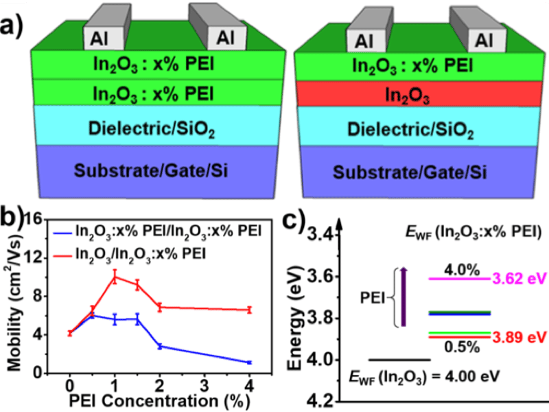
Due to their outstanding electronic properties and high optical transparency, metal oxide thin-film transistors have significant potential in state-of-the-art flat panel display technologies. Here, high performance solution-processed metal oxide thin-film transistors were realized by fabricating heterojunctions of indium oxide (In2O3) and polyethylenimine (PEI) as the semiconducting channel layer. Due to the tunable work function of the In2O3-PEI blends, electron mobilities as high as ~10 cm2V-1s-1 were obtained.
Jun 5, 2018
Northwestern University
Amorphous to Crystalline Transition in Indium Oxide Semiconductors
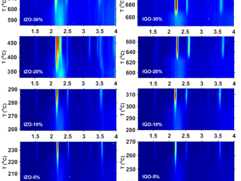
Amorphous oxide semiconductors commonly are indium oxides doped with other metal ions. Although it is known that the introduction of secondary metal ions decreases the degree of crystallinity and elevates the crystallization temperature, there is a lack of systematic study to compare and quantify the effects of different dopant elements. In an interdisciplinary study within IRG-2 of the Northwestern University MRSEC, in situ synchrotron X-ray characterization was performed to characterize the isochronal crystallization process of oxide thin films synthesized by pulsed laser deposition.
Showing 381 to 390 of 1397