Highlights
Jun 13, 2017
University of Wisconsin - Madison
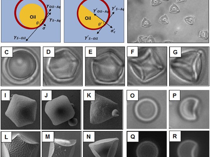
Synthesis of Non-Spherical Particles using Partially-Filled Polymeric Shells
N. L. Abbott, D. M. Lynn; University of Wisconsin-Madison
Spherical particles are easy to synthesize because a sphere is a shape that minimizes surface area. Non-spherical particles, however, have properties that can be very different from spherical particles, but they are challenging to fabricate.
Jun 13, 2017
Northwestern University
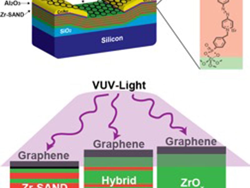
Radiation-Hard Graphene Electronic Devices via Hybrid Dielectrics
Mark Hersam and Tobin Marks, Northwestern University MRSEC
Solution-processed semiconductor and dielectric materials are attractive for satellite technology due to their light-weight, low-voltage operation, and mechanical robustness, but their response to ionizing radiation environments is not well understood.
Jun 13, 2017
Northwestern University
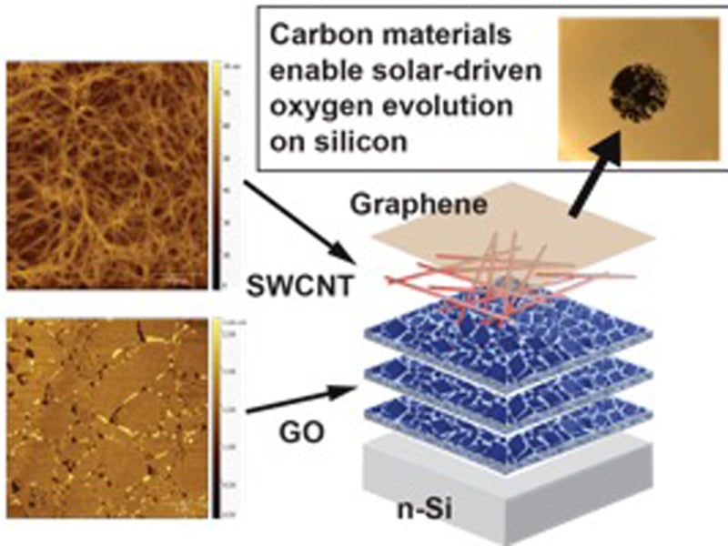
Metal-Free Carbon-Based Nanomaterial Coatings Protect Silicon Photoanodes in Solar Water-Splitting
Solar water splitting converts solar energy into chemical fuels that can be easily stored and transported. Silicon is already used on a large scale for photovoltaics, but it is unstable in the electrolytes used for water oxidation.
Jun 13, 2017
Northwestern University
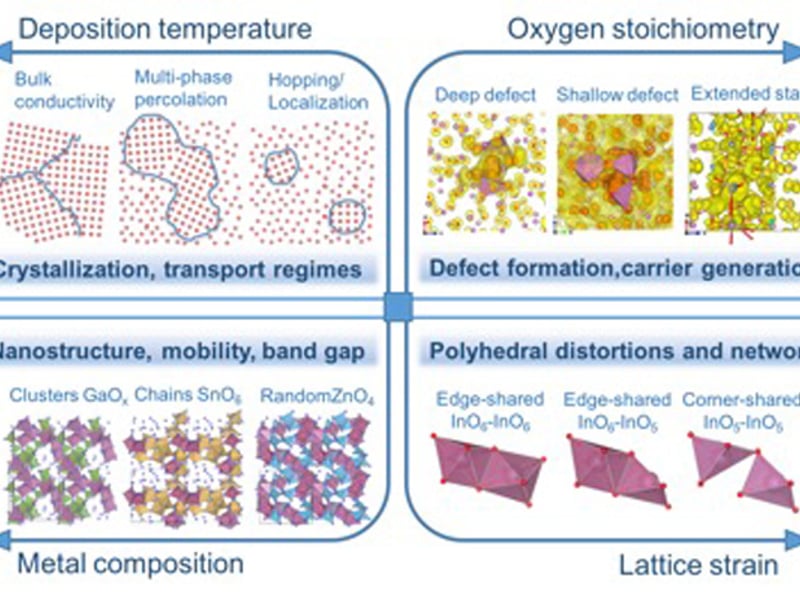
Parameter Space for Amorphous Oxide Semiconductors (AOSs)
Julia Medvedeva and Robert Chang, Northwestern University MRSEC
The combined results of controlled synthesis, ab-initio molecular-dynamics liquid-quench simulations, thorough structure and property characterization, and accurate density-functional calculations helped identify four major components that govern the electrical, optical, thermal, and mechanical properties of prototype In-based AOSs: (i) deposition temperature; (ii) oxygen stoichiometry; (iii) cation composition; and (iv) lattice strain, Figure.
Jun 13, 2017
Northwestern University
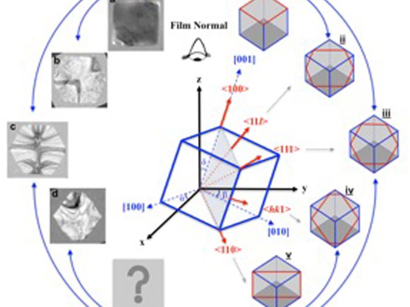
In-situ Crystallization and Morphological Evolution in Multicomponent Indium Oxide Thin Films
Peter Voorhees and Vinayak Dravid, Northwestern University MRSEC
Among all Transparent conducting oxides, Zinc-Indium-Tin Oxides are known for their good chemical stability, smooth surfaces and most importantly, high electrical conductivity. Having access to fundamental information like kinetics parameters is extremely important for processing and fabrication of these materials.
Jun 13, 2017
Northwestern University
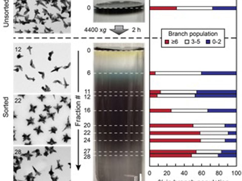
Homogeneous Gold Nanostars
Mark Hersam and Teri Odom, Northwestern University MRSEC
Anisotropic gold nanoparticles have been shown to possess desirable plasmonic and optical properties at the single particle level, but ensemble averaged measurements are compromised by the as-synthesized polydispersity in nanoparticle size and shape.
Jun 13, 2017
Northwestern University
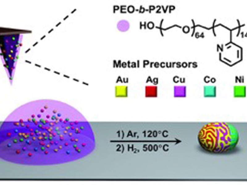
Polyelemental Nanoparticle Libraries
M. Hersam, V. Dravid, C. Mirkin, Northwestern University MRSEC
Multimetallic nanoparticles are useful in many fields, yet there are no effective strategies for synthesizing libraries of such structures with systematic compositional tunability.
Jun 13, 2017
Northwestern University
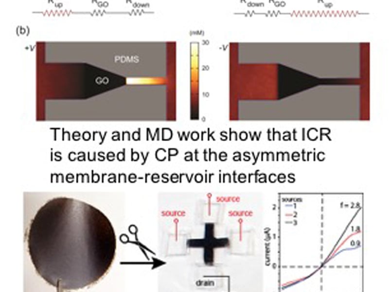
Kirigami Nanofluidics
J. Huang, E. Luijten, M. Olvera de la Cruz, Northwestern University MRSEC
Restacked films of exfoliated 2D nanosheets can function as massive nanofluidic channel arrays. Recent research shows that cutting such membranes into asymmetric shapes leads to ionic current rectification.
Jun 12, 2017
Northwestern University
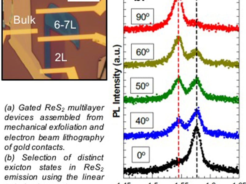
Anisotropic Polarized Emission from ReS2
Nathaniel P. Stern, Northwestern University MRSEC
Optical properties of layered materials can be controlled manipulating the discrete number of atomically-thin two-dimensional crystal layers. Unique amongst the layered transition metal dichalcogenides, ReS2 has optical emission that is linearly polarized and proportional to layer number.

Jun 12, 2017
Northwestern University
Tinkering Lab at Chicago Children's Museum
Northwestern University with the Chicago Children’s Museum in prototyping and formative evaluation of the new permanent exhibit, Tinkering Lab, which focuses on the self-guided exploration of materials for K-8 students.
Showing 541 to 550 of 1452