Highlights

May 25, 2016
Yale University
Electrocatalytic Surfaces Using Bulk Metallic Glass Nanostructures
Osuji, Schroers, and Taylor
Metallic glass nanostructures provide a new platform for electrocatalytic applications. Several surface modification strategies that remove or add metal species (top images) improve the catalytic activity of metallic glass nanostructures. These strategies were demonstrated for three key electrocatalytic reactions important for renewable energy.
May 18, 2016
University of Utah
Leveraging MRSEC Equipment Purchases
Ian R. Harvey, Shared Facilities Director, Utah MRSEC, University of Utah
Leveraged
upgrades to Scanning Transmission Electron Microscope (S/TEM) and Focused Ion
Beam System (FIB):
May 18, 2016
University of Utah
Modeling the UV Electromagnetic Response of Al and Mg Plasmonic Nanostructures
Steve Blair, Department of Computer and Electric Engineering, University of Utah Sivaraman Guruswamy, Department of Metallurgical Engineering, University of Utah
Objective:
Compare the UV plasmonic response of Al and Mg nanostructures. Light
transmission through sub-wavelength aperture arrays shows significant
May 13, 2016
University of Wisconsin - Madison
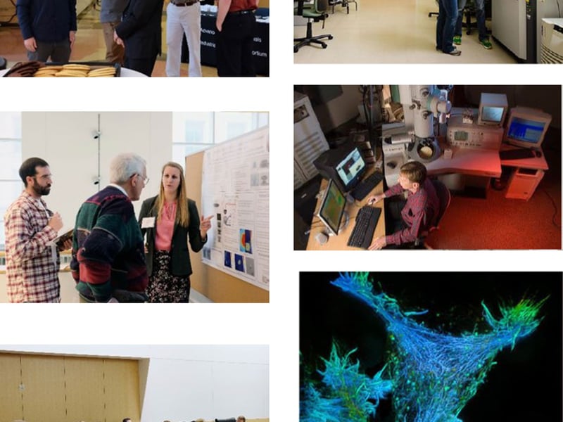
MRSEC Shared Facilities: A Vital Resource
Jerry Hunter, University of Wisconsin-Madison
The resources of the Wisconsin MRSEC Shared Facilities impact researchers campus-wide and beyond. Over the past year >79,000 usage hours accounted for:

May 13, 2016
University of Wisconsin - Madison
Wisconsin MRSEC Outreach Impacts 255,000 People This Year!
Anne Lynn Gillian-Daniel, Benjamin Taylor University of Wisconsin-Madison
Since 2011, the Wisconsin MRSEC has created over 40 unique research-inspired education resources. These resources are disseminated through educational kits, outreach activities, instructional videos and other online resources, all based on cutting-edge research going on in the Wisconsin MRSEC.
These resources have impacted:
>650,000 people in 194 countries.
Over the last year:
May 13, 2016
University of Wisconsin - Madison
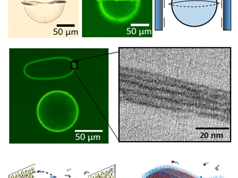
Templating Nanomaterials from Defects in Liquid Crystals
Nicholas L. Abbott, Juan J. de Pablo*, University of Wisconsin-Madison, *University of Chicago
Defects in liquid crystals can function as nanoscopic molds for assembling molecules
May 13, 2016
University of Wisconsin - Madison
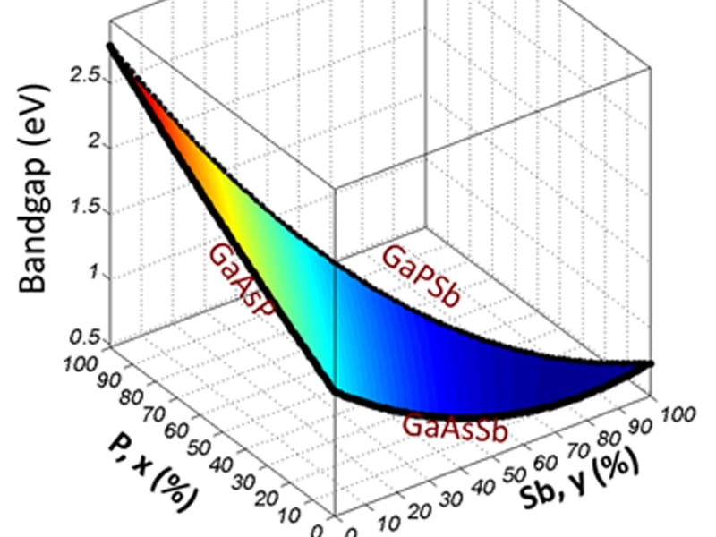
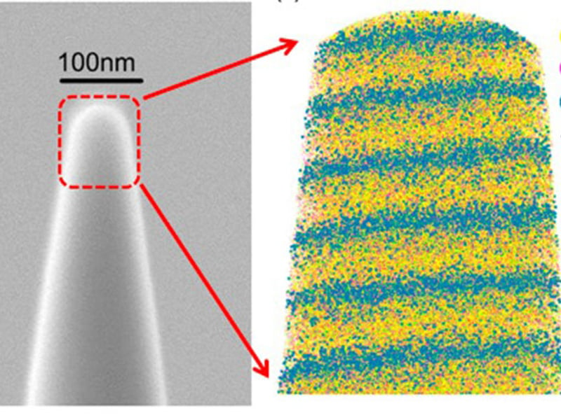
Full Circle of Innovation in Instrumentation: Atomic Level Imaging
Susan E. Babcock, Thomas F. Kuech, University of Wisconsin-Madison
A MRSEC innovation comes back home to reveal the atomic structure of new materials
May 5, 2016
University of Minnesota - Twin Cities
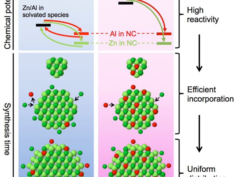
Efficient and uniform doping of zinc oxide nanocrystals via plasma synthesis
Eray Aydil, Uwe Kortshagen, Andre Mkhoyan
In solution-based synthesis, often doping efficiencies are low and dopants are excluded from the nanocrystals’ central cores. The research team developed a fundamentally different plasma-based process for synthesizing aluminum-doped zinc oxide nanocrystals.
May 4, 2016
University of Minnesota - Twin Cities
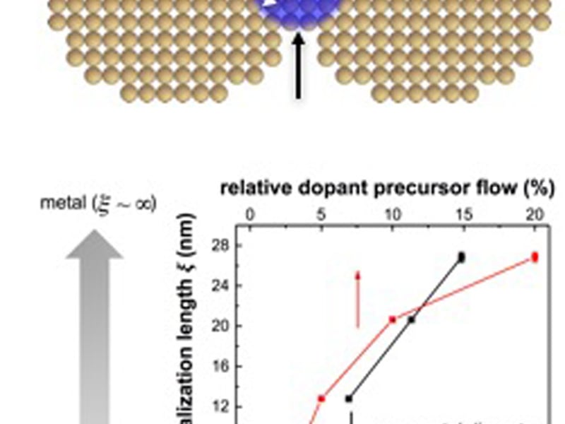
How many electrons make a nanocrystal film metallic?
Uwe Kortshagen, Boris Shklovskii (IRG-2)
Understanding the transport of electrons in films of touching nanocrystals is of central importance for their future use in printed electronic devices such as light emitting diodes, solar cells, or transistors. The research team developed a new theory that describes the transition of the electron conduction in doped nanocrystal films from a semiconducting to a metallic behavior.
Showing 551 to 560 of 1397